Difference: TCADIrradSurfaceDamage (1 vs. 2)
Revision 22018-08-28 - AtlasjSilicon
| |||||||||||
| Changed: | |||||||||||
| < < | Title表面電荷のシミュレーション | ||||||||||
| > > | TCAD 表面電荷のシミュレーション | ||||||||||
SDEVICE編集 | |||||||||||
| Changed: | |||||||||||
| < < | 電荷を置くには,sdevice_des.cmdに下のようなPhysicsの項目を足します. | ||||||||||
| > > | 基本的な情報はmanual/sdevice_ug.pdf/chapter17にあります. | ||||||||||
| Added: | |||||||||||
| > > | bulk damageやsurface damageについて書いてありますが,ここでは表面電荷の置き方について. 電荷を置くには,sdevice_des.cmdに下のようなPhysicsの項目を足します. | ||||||||||
Physics (Material="Oxide"){
    Charge (Conc=<float>[cm-3])
}
Materialの所は,Material / Region / MaterialInterface / RegionInterface に変えられます. | |||||||||||
| Changed: | |||||||||||
| < < | Interfaceの場合は下のように2つのMaterialをスラッシュで区切って指定します. | ||||||||||
| > > | 因みにbulk damageの場合はChargeの所がTrapsになりますが,どこの領域かを指定する初めの所は共通です. | ||||||||||
| Added: | |||||||||||
| > > | Interfaceの場合は下のように2つのMaterialをスラッシュで区切って指定します. | ||||||||||
Physics (MaterialInterface="Oxide/Silicon"){
    Charge (Uniform (or) Gaussian
          Conc=<float>[cm-2]
          SpaceMid=<vector>[um]
          SpaceSig=<vector>[um])
}
MateirialやRegionで領域を指定した場合は,変数はConc(concentration)のみ.
Interfaceを指定した場合はUniformならConcのみ.GaussianならSpaceMid/SpaceSigを指定して分布を決定. | |||||||||||
| Added: | |||||||||||
| > > | Gaussianの中心値の座標をSpaceMidで指定し,自分で決めた1σ分離れた座標をSpaceSigで指定します.
concentrationを実際にどの程度に設定するべきかは調査中です.
次に示す例ではちょうど変化が見える値を採用しています.
ダイオードの例下のようなダイオードを用意しました. sde file : /home/swada/work/Sentaurus/TCAD_WS_2/sde_dvs.cmd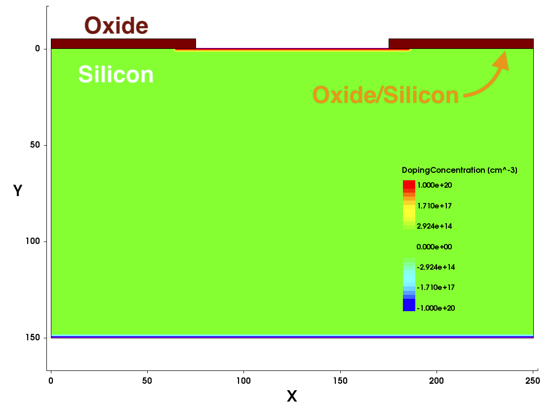 上から酸化膜(Oxide),n+電極(P:1e+20),p bulk(B:1e+12),p+電極(B:1e+20).
sdeviceに
上から酸化膜(Oxide),n+電極(P:1e+20),p bulk(B:1e+12),p+電極(B:1e+20).
sdeviceに
Physics (MaterialInterface="Oxide/Silicon") {
 Charge(Conc=2.5e10)
}
を書く前後でIVシミュレーションを行い,eDencity分布を比較します.
前 sdevice file : /home/swada/work/Sentaurus/TCAD_WS_2/IV_des.cmd
後 sdevice file : /home/swada/work/Sentaurus/TCAD_WS_2/IVirrad_des.cmd
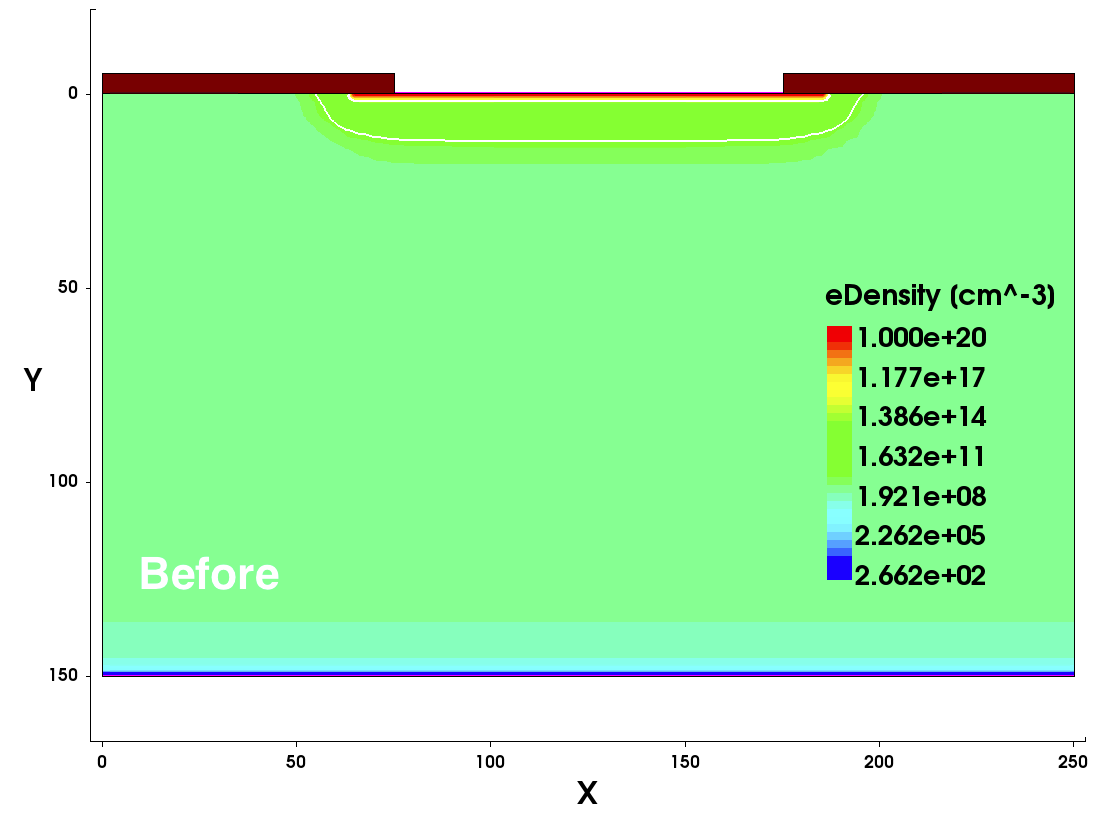 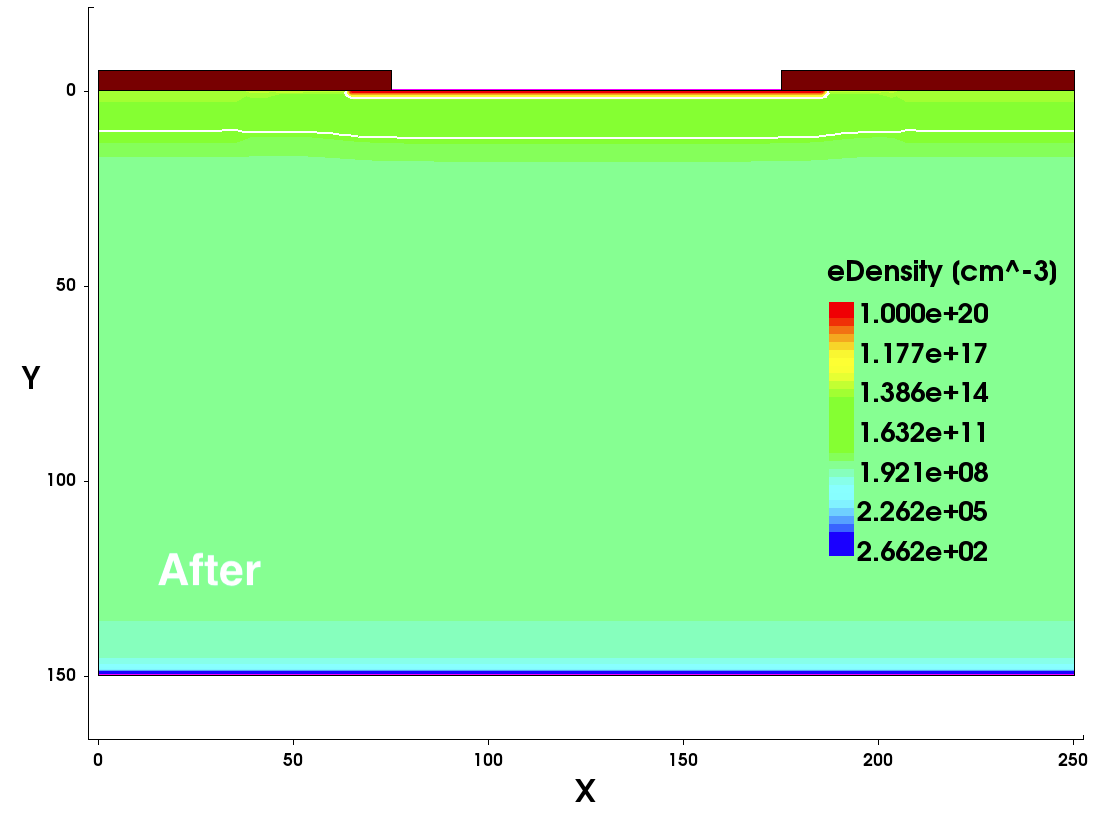 Oxide/Silicon境界にプラス電荷を置いたため,境界に電子が集まっているのが見えます.
CVシミュレーションについても同様にsdevice fileを用意しました.
前 sdevice file : /home/swada/work/Sentaurus/TCAD_WS_2/CV_des.cmd
後 sdevice file : /home/swada/work/Sentaurus/TCAD_WS_2/CVirrad_des.cmd
IV測定とCV測定の結果を前後で比較してみます.
Oxide/Silicon境界にプラス電荷を置いたため,境界に電子が集まっているのが見えます.
CVシミュレーションについても同様にsdevice fileを用意しました.
前 sdevice file : /home/swada/work/Sentaurus/TCAD_WS_2/CV_des.cmd
後 sdevice file : /home/swada/work/Sentaurus/TCAD_WS_2/CVirrad_des.cmd
IV測定とCV測定の結果を前後で比較してみます.
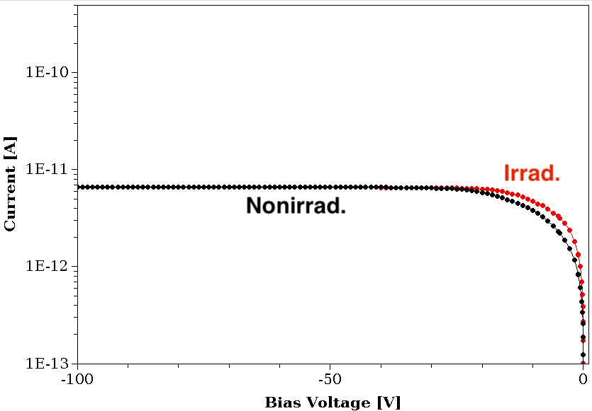  電荷を置いたことによって変化が生じているのが分かります.
 | ||||||||||
-- Comments | |||||||||||
| Added: | |||||||||||
| > > |
| ||||||||||
Revision 12018-08-28 - AtlasjSilicon
Title表面電荷のシミュレーションSDEVICE編集電荷を置くには,sdevice_des.cmdに下のようなPhysicsの項目を足します.Physics (Material="Oxide"){
Charge (Conc=<float>[cm-3])
}
Materialの所は,Material / Region / MaterialInterface / RegionInterface に変えられます.
Interfaceの場合は下のように2つのMaterialをスラッシュで区切って指定します.
Physics (MaterialInterface="Oxide/Silicon"){
    Charge (Uniform (or) Gaussian
          Conc=<float>[cm-2]
          SpaceMid=<vector>[um]
          SpaceSig=<vector>[um])
}
MateirialやRegionで領域を指定した場合は,変数はConc(concentration)のみ.
Interfaceを指定した場合はUniformならConcのみ.GaussianならSpaceMid/SpaceSigを指定して分布を決定.
-- Comments |
View topic | History: r2 < r1 | More topic actions...
Ideas, requests, problems regarding TWiki? Send feedback